
Introduction
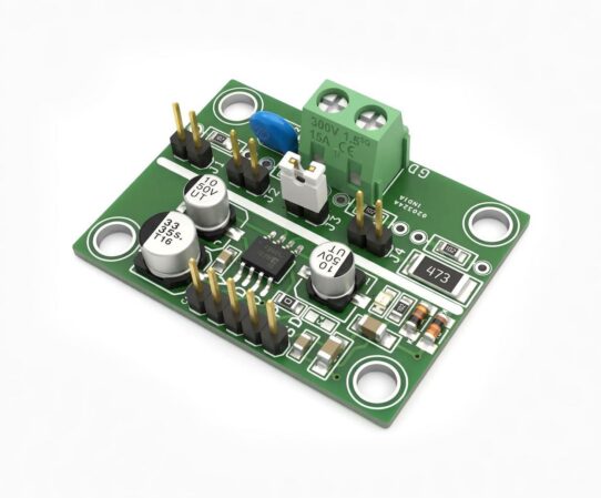
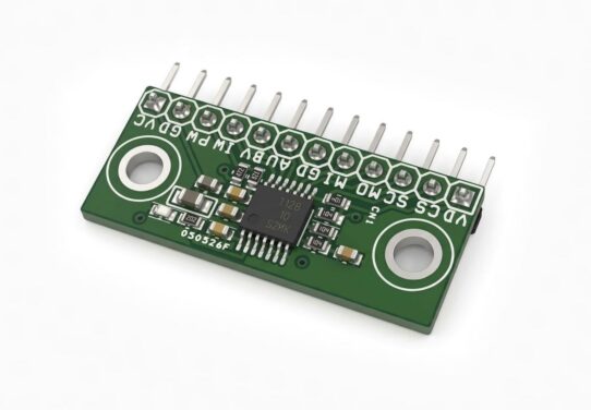
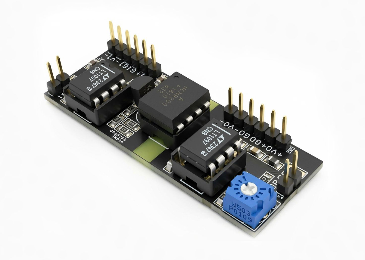
This project is a high-precision analog isolation amplifier designed for accurate signal transmission across an isolation barrier while providing complete galvanic isolation between the input and output circuits. It is an excellent solution for industrial control systems, high-voltage measurement, sensor interfaces, battery management systems, and other applications where electrical isolation and high measurement accuracy are essential.
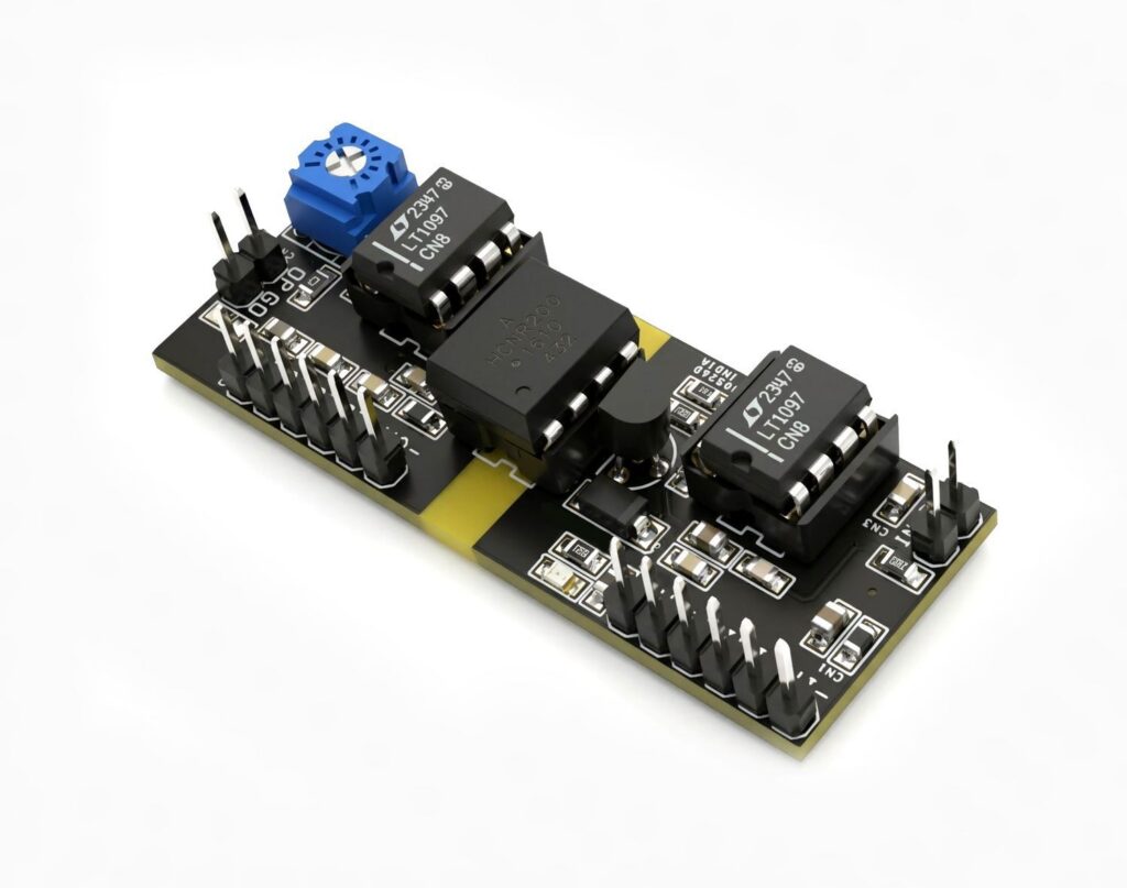
The circuit achieves its high accuracy and wide dynamic range by combining the HCNR200 linear optocoupler with two LT1097 precision operational amplifiers, which feature extremely low input offset voltage and low input bias current. The overall performance of the circuit is primarily determined by the characteristics of the HCNR200 optocoupler.
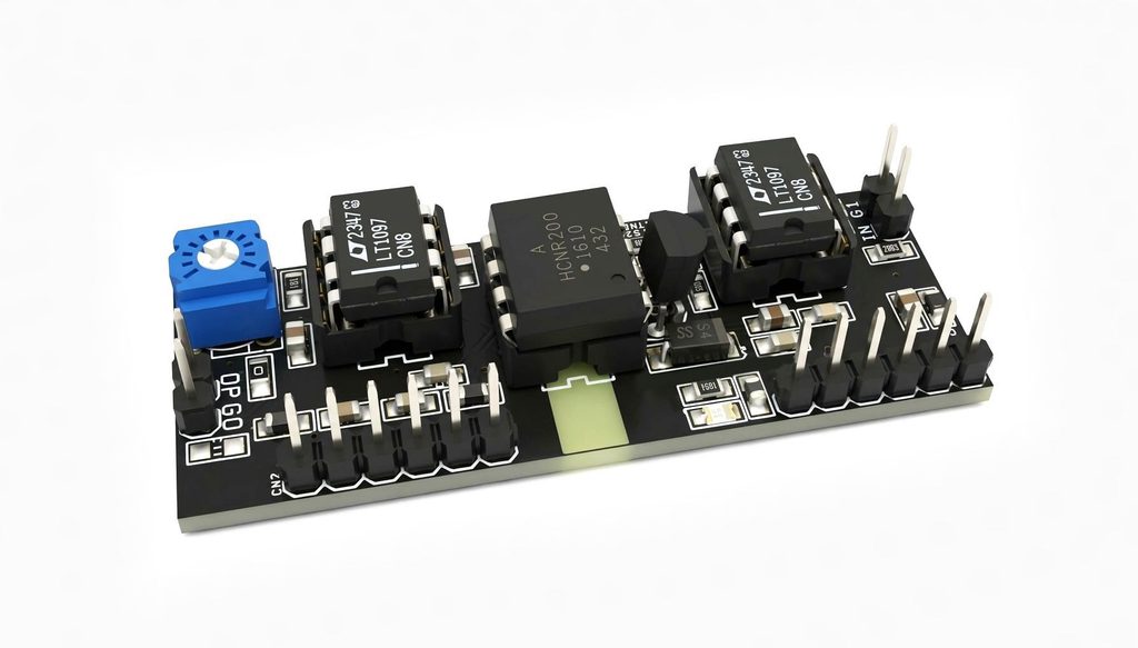
The amplifier is designed to accurately process analog input and output signals from 1 mV to 10 V, making it suitable for both low-level sensor signals and higher voltage analog interfaces.
Features
- High-precision analog signal isolation
- Complete galvanic isolation between input and output
- Input/output voltage range: 1 mV to 10 V
- Based on HCNR200 linear optocoupler and LT1097 precision op-amps
- Typical bandwidth of approximately 10 kHz
- Low offset voltage and excellent linearity
- Adjustable unity gain using an onboard 50 kΩ trimmer
- No offset calibration required
- Kelvin-connected photodiodes and op-amp inputs for improved accuracy
- Low output noise with stable compensated feedback loops
- Ideal for industrial control, sensor isolation, high-voltage measurement, battery monitoring, and data acquisition system
- Supply +/-15V Input Side
- Supply +/-15V Output Side
- On Board Power LED Input Side
- High-Linearity
- Ferrite Bead on Power Line for noise protection
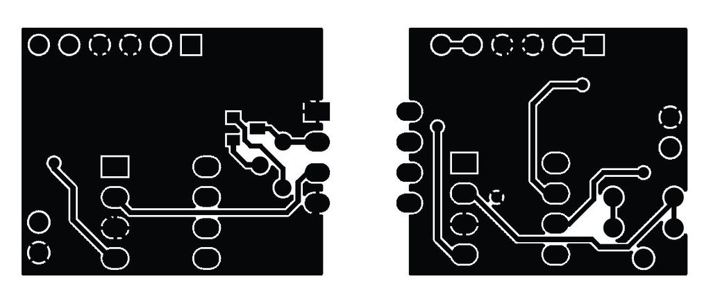
- PCB Dimensions 55.72 x 20.96 mm
Schematic
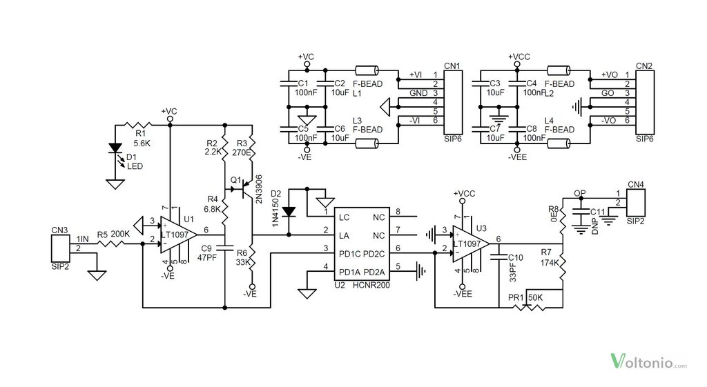
Connections
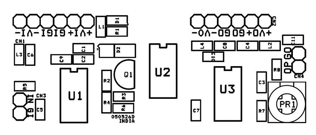
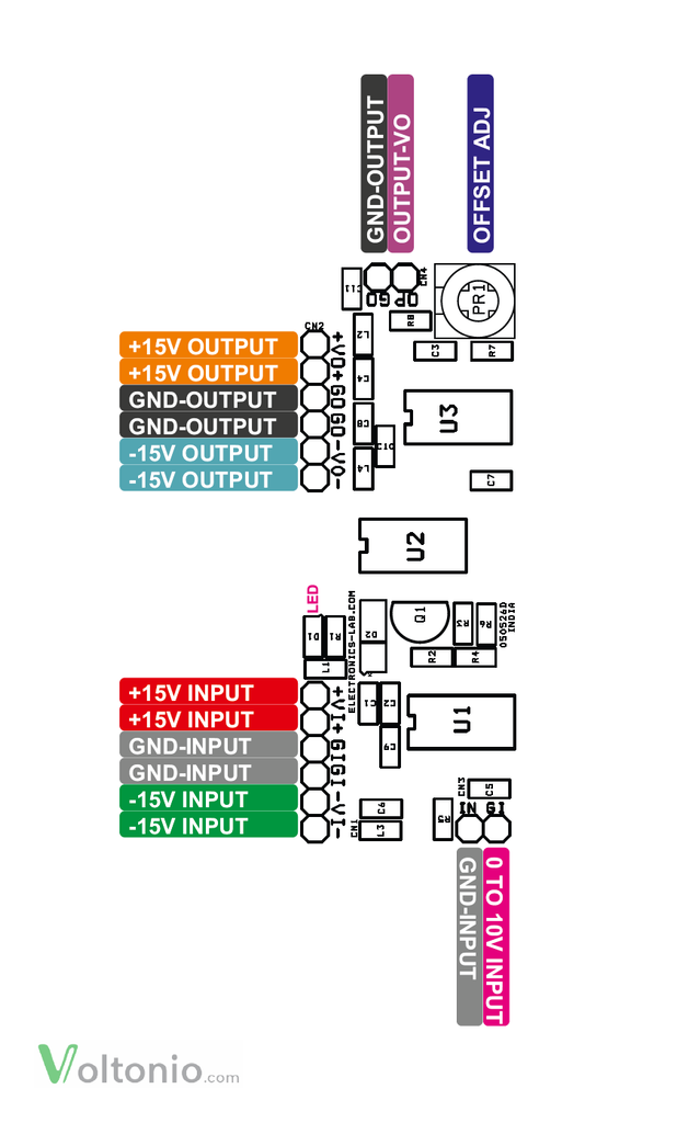
- CN1: Pin 1,2 = +15V DC Input Side, Pin 3,4 = GND Input Side, Pin 5.6 = -15V Input Side
- CN2: Pin 1,2 = +15V Output Side, Pin 3,4 = GND Output Side, Pin 5,6 = -15V Output Side
- CN3: Pin 1 = Input Voltage 0 to 10V, Pin 2 = GND-Input
- CN4: Pin 1 = Output Voltage 0 to 10V, Pin 2 = GND-Output
- PR1: Pre-set for Offset Adjust
- D1: Power LED Input Side
Part List
| NO. | QNTY. | REF. | DESC. | MANUFACTURER | SUPPLIER | SUPPLIER PART NO |
|---|---|---|---|---|---|---|
| 1 | 2 | CN1,CN2 | 6 PIN MALE HEADER PITCH 2.54MM | WURTH | DIGIKEY | 732-5319-ND |
| 2 | 2 | CN3,CN4 | 2 PIN MALE HEADER PITCH 2.54MM | WURTH | DIGIKEY | 732-5315-ND |
| 3 | 4 | C1,C4,C5,C8 | 100nF/50V CERAMIC SMD SIZE 0805 | YAGEO/MURATA | DIGIKEY | |
| 4 | 4 | C2,C3,C6,C7 | 10uF/25V CERAMIC SMD SIZE 0805 | YAGEO/MURATA | DIGIKEY | |
| 5 | 1 | C9 | 47PF/50V CERAMIC SMD SIZE 0805 | YAGEO/MURATA | DIGIKEY | |
| 6 | 1 | C10 | 33PF/50V CERAMIC SMD SIZE 0805 | YAGEO/MURATA | DIGIKEY | |
| 7 | 1 | C11 | DNP | |||
| 8 | 1 | D1 | LED RED SMD SIZE 0805 | OSRAM | DIGIKEY | 475-1278-1-ND |
| 9 | 1 | D2 | SS14 | ONSEMI | DIGIKEY | SS14CT-ND |
| 10 | 4 | L1,L2,L3,L4 | F-BEAD 600OHM SMD SIZE 0805 | YAGEO/MURATA | DIGIKEY | 240-2390-1-ND |
| 11 | 1 | PR1 | 50K TRIMMER POT | BOURNS INC | DIGIKEY | 3362P-503LF-ND |
| 12 | 1 | Q1 | 2N3906 | ONSEMI | DIGIKEY | 488-2N3906-ND |
| 13 | 1 | R1 | 5.6K 1% SMD SIZE 0805 | YAGEO/MURATA | DIGIKEY | |
| 14 | 1 | R2 | 2.2K 1% SMD SIZE 0805 | YAGEO/MURATA | DIGIKEY | |
| 15 | 1 | R3 | 270E 1% SMD SIZE 0805 | YAGEO/MURATA | DIGIKEY | |
| 16 | 1 | R4 | 6.8K 1% SMD SIZE 0805 | YAGEO/MURATA | DIGIKEY | |
| 17 | 1 | R5 | 200K 1% SMD SIZE 0805 | YAGEO/MURATA | DIGIKEY | |
| 18 | 1 | R6 | 33K 1% SMD SIZE 0805 | YAGEO/MURATA | DIGIKEY | |
| 19 | 1 | R7 | 174K 1% SMD SIZE 0805 | YAGEO/MURATA | DIGIKEY | |
| 20 | 1 | R8 | 0E 5% SMD SIZE 0805 | YAGEO/MURATA | DIGIKEY | |
| 21 | 2 | U1,U3 | LT1097 DIP8 | ANALOG DEVICES | DIGIKEY | 505-LT1097CN8#PBF-ND |
| 22 | 1 | U2 | HCNR200 DIP8 | BROADCOM | DIGIKEY | 516-1522-5-ND |
| 23 | 3 | SOCKET | 8 PIN DIP IC SOCKET | 3M | DIGIKEY | 3M5461-ND |
Circuit Calibration
Stability, Accuracy, and Noise Reduction
To ensure stable operation, the input and output control loops are compensated using capacitors C9 and C10. Rather than reducing the loop gain—which would compromise accuracy—these compensation capacitors improve loop stability while maintaining precision. They also limit the amplifier bandwidth to approximately 10 kHz, helping to reduce output noise. Larger capacitor values may be used if a lower bandwidth and further noise reduction are desired.
The additional LED driver stage, consisting of Q1 and R4–R6, maintains constant LED transconductance over the entire input voltage range. Without this circuitry, the LED drive current would become nonlinear at low input voltages, reducing loop gain and degrading both accuracy and bandwidth. Diode D2 protects the optocoupler LED from excessive reverse voltage when the LED switches off completely.
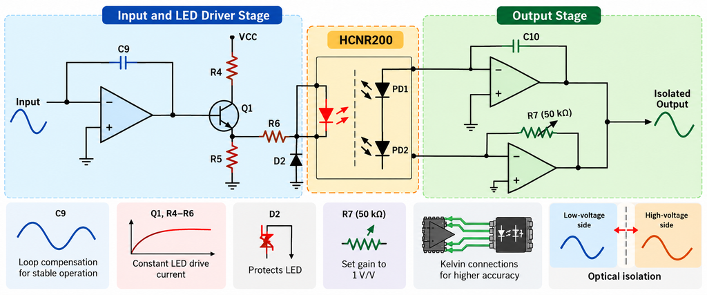
No offset adjustment is required during calibration. The amplifier gain can be accurately set to unity (1 V/V) by adjusting the 50 kΩ trimmer potentiometers incorporated in R7. For maximum measurement accuracy, the op-amp inputs and the HCNR200 photodiodes are connected using Kelvin connections, minimizing errors caused by PCB trace resistance.
This module is an excellent choice for interfacing low-level sensors with high-voltage systems. The complete optical isolation effectively eliminates ground loops, suppresses common-mode noise, protects low-voltage electronics from high-voltage transients, and ensures reliable signal transmission in electrically noisy industrial environments.
HCNR200 Optocoupler
Working Principle and Analog Isolation
The Broadcom® HCNR200 high-linearity analog optocoupler consists of a high-performance AlGaAs LED that illuminates two closely matched photodiodes. The input photodiode monitors, and therefore stabilizes, the light output of the LED. As a result, the nonlinearity and drift characteristics of the LED can be virtually eliminated. The output photodiode produces a photocurrent that is linearly related to the light output of the LED.
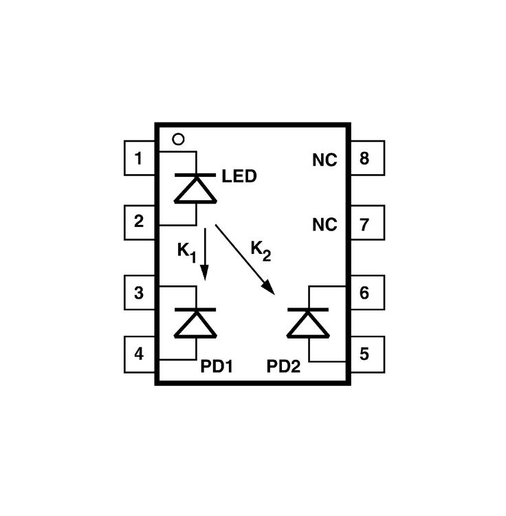
The close matching of the photodiodes and advanced design of the package ensure the high linearity and stable gain characteristics of the optocoupler. The HCNR200/201 isolates analog signals in a wide variety of applications that require good stability, linearity, bandwidth, and low cost. The HCNR200/201 is flexible and, by appropriate design of the application circuit, is capable of operating in many different modes, including unipolar/ bipolar, AC/DC and inverting/noninverting. The HCNR200/201 is an excellent solution for many analog isolation problems.
Figure shows how the HCNR200/201 high linearity optocoupler is configured. The basic optocoupler consists of an LED and two photodiodes. The LED and one of the photodiodes (PD1) are on the input lead frame and the other photodiode (PD2) is on the output lead frame. The package of the optocoupler is constructed so that each photodiode receives approximately the same amount of light from the LED.
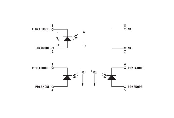
An external feedback amplifier can be used with PD1 to monitor the light output of the LED and automatically adjust the LED current to compensate for any nonlinearities or changes in light output of the LED. The feedback amplifier acts to stabilize and linearize the light output of the LED. The output photodiode then converts the stable, linear light output of the LED into a current, which can then be converted back into a voltage by another amplifier.
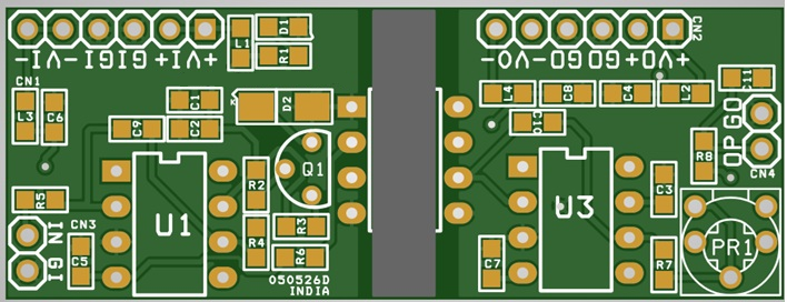
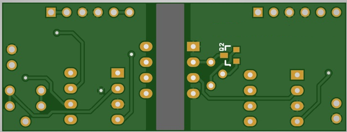
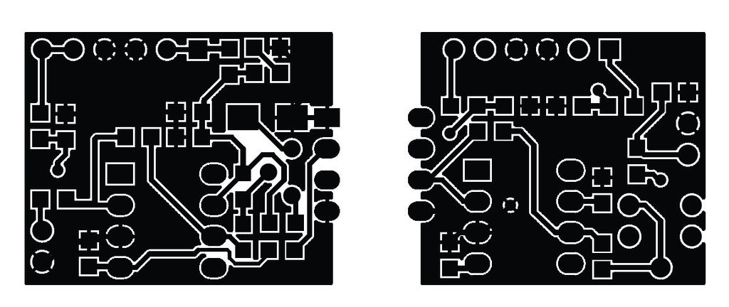
PCB View